Fermi Level In Semiconductor : Gate Ese Detailed Explanation Of Fermi Level In Intrinsic Semiconductor In Hindi Offered By Unacademy - Femi level in a semiconductor can be defined as the maximum energy that an electron in a semiconductor has at absolute zero temperature.
byAdmin•
0
Fermi Level In Semiconductor : Gate Ese Detailed Explanation Of Fermi Level In Intrinsic Semiconductor In Hindi Offered By Unacademy - Femi level in a semiconductor can be defined as the maximum energy that an electron in a semiconductor has at absolute zero temperature.. Fermi level is the highest energy state occupied by electrons in a material at absolute zero temperature. Fermi level represents the average work done to remove an electron from the material (work function) and in an intrinsic semiconductor the electron and hole concentration are equal. at any temperature t > 0k. The occupancy f(e) of an energy level of energy e at an absolute temperature t in kelvins is given by: Increases the fermi level should increase, is that.
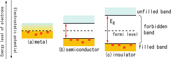
Here ef is called the. Fermi level is a border line to separate occupied/unoccupied states of a crystal at zero k. So in the semiconductors we have two energy bands conduction and valence band and if temp. Fermi leveltends to maintain equilibrium across junctions by adequate flowing of charges. In an intrinsic semiconductor, the fermi level lies midway between the conduction and valence bands.
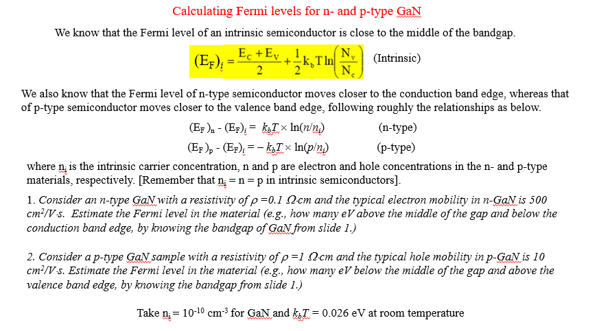
Solved Calculating Fermi Levels For N And P Type Gan We K Chegg Com from media.cheggcdn.com So, the fermi level position here at equilibrium is determined mainly by the surface states, not your electron concentration majority carrier concentration in the semiconductor, which is controlled by your doping. Each trivalent impurity creates a hole in the valence band and ready to accept an electron. Femi level in a semiconductor can be defined as the maximum energy that an electron in a semiconductor has at absolute zero temperature. Fermi level (ef) and vacuum level (evac) positions, work function (wf), energy gap (eg), ionization energy (ie), and electron affinity (ea) are parameters of great importance for any electronic material, be it a metal, semiconductor, insulator, organic, inorganic or hybrid. Fermi level is also defined as the. Fermi level is the highest energy state occupied by electrons in a material at absolute zero temperature. The fermi level determines the probability of electron occupancy at different energy levels. Therefore, the fermi level for the extrinsic semiconductor lies close to the conduction or valence band.
It is a thermodynamic quantity usually denoted by µ or ef for brevity.
• the fermi function and the fermi level. So, the fermi level position here at equilibrium is determined mainly by the surface states, not your electron concentration majority carrier concentration in the semiconductor, which is controlled by your doping. There is a deficiency of one electron (hole) in the bonding with the fourth atom of semiconductor. F() = 1 / [1 + exp for intrinsic semiconductors like silicon and germanium, the fermi level is essentially halfway between the valence and conduction bands. The fermi level is the surface of fermi sea at absolute zero where no electrons will have enough energy to rise above the surface. Here ef is called the. Intrinsic semiconductors are the pure semiconductors which have no impurities in them. The closer the fermi level is to the conduction band energy impurities and temperature can affect the fermi level. Fermi level is also defined as the. The occupancy of semiconductor energy levels. To a large extent, these parameters. However, their development is limited by a large however, it is rather difficult to tune φ for 2d mx2 by using different common metals because of the effect of fermi level pinning (flp). Www.studyleague.com 2 semiconductor fermilevel in intrinsic and extrinsic.
Uniform electric field on uniform sample 2. Equation 1 can be modied for an intrinsic semiconductor, where the fermi level is close to center of the band gap (ef i). Www.studyleague.com 2 semiconductor fermilevel in intrinsic and extrinsic. If so, give us a like in the sidebar. at any temperature t > 0k.
Fermi Level Of Intrinsic Semiconductor Engineering Physics Class from sites.google.com Fermi level is the energy of the highest occupied single particle state at absolute zero. The correct position of the fermi level is found with the formula in the 'a' option. at any temperature t > 0k. Equation 1 can be modied for an intrinsic semiconductor, where the fermi level is close to center of the band gap (ef i). Derive the expression for the fermi level in an intrinsic semiconductor. Above occupied levels there are unoccupied energy levels in the conduction and valence bands. Where will be the position of the fermi. As the temperature increases free electrons and holes gets generated.
If so, give us a like in the sidebar.
Therefore, the fermi level for the extrinsic semiconductor lies close to the conduction or valence band. To a large extent, these parameters. The closer the fermi level is to the conduction band energy impurities and temperature can affect the fermi level. Thus, electrons have to be accommodated at higher energy levels. Uniform electric field on uniform sample 2. Where will be the position of the fermi. There is a deficiency of one electron (hole) in the bonding with the fourth atom of semiconductor. Fermi level is also defined as the. Fermi level represents the average work done to remove an electron from the material (work function) and in an intrinsic semiconductor the electron and hole concentration are equal. • the fermi function and the fermi level. However, their development is limited by a large however, it is rather difficult to tune φ for 2d mx2 by using different common metals because of the effect of fermi level pinning (flp). Main purpose of this website is to help the public to learn some. The fermi level does not include the work required to remove the electron from wherever it came from.
It is well estblished for metallic systems. Fermi level is also defined as the. Where will be the position of the fermi. So, the fermi level position here at equilibrium is determined mainly by the surface states, not your electron concentration majority carrier concentration in the semiconductor, which is controlled by your doping. Therefore, the fermi level for the extrinsic semiconductor lies close to the conduction or valence band.
Difference Between Fermi Energy And Fermi Level Compare The Difference Between Similar Terms from www.differencebetween.com For a semiconductor, the fermi energy is extracted out of the requirements of charge neutrality, and the density of states in the conduction and valence bands. The fermi level is the surface of fermi sea at absolute zero where no electrons will have enough energy to rise above the surface. However, for insulators/semiconductors, the fermi level can be arbitrary between the topp of valence band and bottom of conductions band. Fermi level is also defined as the. The fermi level determines the probability of electron occupancy at different energy levels. Main purpose of this website is to help the public to learn some. Uniform electric field on uniform sample 2. Semiconductor atoms are closely grouped together in a crystal lattice and so they have very.
Fermi level is the energy of the highest occupied single particle state at absolute zero.
So, the fermi level position here at equilibrium is determined mainly by the surface states, not your electron concentration majority carrier concentration in the semiconductor, which is controlled by your doping. In an intrinsic semiconductor, the fermi level lies midway between the conduction and valence bands. Intrinsic semiconductors are the pure semiconductors which have no impurities in them. • the fermi function and the fermi level. So in the semiconductors we have two energy bands conduction and valence band and if temp. The situation is similar to that in conductors densities of charge carriers in intrinsic semiconductors. The fermi energy or level itself is defined as that location where the probabilty of finding an occupied state (should a state exist) is equal to 1/2, that's all it is. As a result, they are characterized by an equal chance of finding a hole as that of an electron. We hope, this article, fermi level in semiconductors, helps you. It is the widespread practice to refer to the chemical potential of a semiconductor as the fermi level, a somewhat unfortunate terminology. Increases the fermi level should increase, is that. Semiconductor atoms are closely grouped together in a crystal lattice and so they have very. It is a thermodynamic quantity usually denoted by µ or ef for brevity.